Fermi Level In Semiconductor - 7: Illustrated scheme showing the Fermi level position ... : Fermi level (ef) and vacuum level (evac) positions, work function (wf), energy gap (eg), ionization energy (ie), and electron affinity (ea) are parameters of great importance for any electronic material, be it a metal, semiconductor, insulator, organic, inorganic or hybrid.
Fermi Level In Semiconductor - 7: Illustrated scheme showing the Fermi level position ... : Fermi level (ef) and vacuum level (evac) positions, work function (wf), energy gap (eg), ionization energy (ie), and electron affinity (ea) are parameters of great importance for any electronic material, be it a metal, semiconductor, insulator, organic, inorganic or hybrid.. Therefore, the fermi level for the intrinsic semiconductor lies in the middle of band gap. Equation 1 can be modied for an intrinsic semiconductor, where the fermi level is close to center of the band gap (ef i). Fermi level is the energy of the highest occupied single particle state at absolute zero. Each trivalent impurity creates a hole in the valence band and ready to accept an electron. It is a thermodynamic quantity usually denoted by µ or ef for brevity.
If so, give us a like in the sidebar. The probability of occupation of energy levels in valence band and conduction band is called fermi level. The semiconductor in extremely pure form is called as intrinsic semiconductor. We hope, this article, fermi level in semiconductors, helps you. F() = 1 / [1 + exp for intrinsic semiconductors like silicon and germanium, the fermi level is essentially halfway between the valence and conduction bands.
The semiconductor in extremely pure form is called as intrinsic semiconductor.
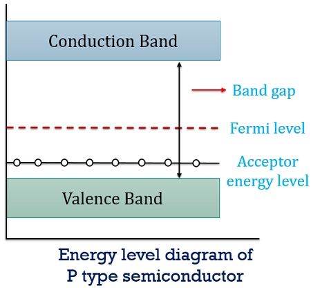
Fermi level (ef) and vacuum level (evac) positions, work function (wf), energy gap (eg), ionization energy (ie), and electron affinity (ea) are parameters of great importance for any electronic material, be it a metal, semiconductor, insulator, organic, inorganic or hybrid. Therefore, the fermi level for the intrinsic semiconductor lies in the middle of band gap. Where will be the position of the fermi. Uniform electric field on uniform sample 2. Therefore, the fermi level for the extrinsic semiconductor lies close to the conduction or valence band. It is the oldest practical. • the fermi function and the fermi level. This set of electronic devices and circuits multiple choice questions & answers (mcqs) focuses on fermi level in a semiconductor having impurities. Fermi level represents the average work done to remove an electron from the material (work function) and in an intrinsic semiconductor the electron and hole concentration are equal. Those semi conductors in which impurities. If so, give us a like in the sidebar. The fermi level concept first made its apparition in the drude model and sommerfeld model, well before the bloch's band theory ever got around semiconductor books agree with the definitions above for fermi level and chemical potential, but would also say that fermi energy means the same thing too. Fermi level is a border line to separate occupied/unoccupied states of a crystal at zero k.
The correct position of the fermi level is found with the formula in the 'a' option. Tersoff, schottky barrier heights and the continuum of gap states, phys. Each trivalent impurity creates a hole in the valence band and ready to accept an electron. The fermi level (i.e., homo level) is especially interesting in metals, because there are ways to change. Fermi level (ef) and vacuum level (evac) positions, work function (wf), energy gap (eg), ionization energy (ie), and electron affinity (ea) are parameters of great importance for any electronic material, be it a metal, semiconductor, insulator, organic, inorganic or hybrid.
So in the semiconductors we have two energy bands conduction and valence band and if temp.
In this module on metal semiconductor contacts, we will cover the following topics: In all cases, the position was essentially independent of the metal. (ii) fermi energy level : The fermi level is the surface of fermi sea at absolute zero where no electrons will have enough energy to rise above the surface. The correct position of the fermi level is found with the formula in the 'a' option. Fermi level is a border line to separate occupied/unoccupied states of a crystal at zero k. Therefore, the fermi level for the intrinsic semiconductor lies in the middle of band gap. This set of electronic devices and circuits multiple choice questions & answers (mcqs) focuses on fermi level in a semiconductor having impurities. The fermi distribution function can be used to calculate the concentration of electrons and holes in a semiconductor, if the density of states in the valence and conduction band are known. It is well estblished for metallic systems. Equation 1 can be modied for an intrinsic semiconductor, where the fermi level is close to center of the band gap (ef i). Uniform electric field on uniform sample 2. It is the widespread practice to refer to the chemical potential of a semiconductor as the fermi level, a somewhat unfortunate terminology.
It is the oldest practical. The fermi level is the surface of fermi sea at absolute zero where no electrons will have enough energy to rise above the surface. Position is directly proportional to the logarithm of donor or acceptor concentration it is given by The fermi level does not include the work required to remove the electron from wherever it came from. Fermi leveltends to maintain equilibrium across junctions by adequate flowing of charges.

It is well estblished for metallic systems.
We hope, this article, fermi level in semiconductors, helps you. Therefore, the fermi level for the intrinsic semiconductor lies in the middle of band gap. Документы, похожие на «5.fermi level in itrinsic and extrinsic semiconductor». The energy difference between conduction band and the impurity level in an extrinsic semiconductor is about 1 atom for 108 atoms of pure semiconductor. in either material, the shift of fermi level from the central. Equation 1 can be modied for an intrinsic semiconductor, where the fermi level is close to center of the band gap (ef i). The band theory of solids gives the picture that there is a sizable gap between the fermi level and the conduction band of the semiconductor. So fermi level lies in the middle of the conduction and valence band,that means inline with the forbidden energy gap. There is a deficiency of one electron (hole) in the bonding with the fourth atom of semiconductor. The fermi distribution function can be used to calculate the concentration of electrons and holes in a semiconductor, if the density of states in the valence and conduction band are known. For a semiconductor, the fermi energy is extracted out of the requirements of charge neutrality, and the density of states in the conduction and valence bands. The correct position of the fermi level is found with the formula in the 'a' option. To a large extent, these parameters.


Komentar
Posting Komentar